


By Pradeep Chakraborty
Last year, edge-emitting lasers (EELs) had represented a US$2.5 billion market, according to France’s Yole Développement (Yole), in its technology and market analysis. EELs are mainly used in optical communications, with optical systems for datacom and telecom.
Martin Vallo, Technology & Market Analyst at Yole Développement, France, said: “Growth is still driven by the optical communication market segment with optical systems for datacom and telecom. It is today the largest EELs segment with 56 percent of the total revenue in 2018.” The potential market size for EELs in future, is said to be worth $4.6 billion for 2023 at a CAGR of 13 percent.
Killer apps
Let’s find out the traditional applications that are still driving the EEL market. He said: “Growth of EEL market will continue to be driven by the optical communication segment, such as optical systems for datacom and telecom. This is the largest segment today for EELs, comprising 56 percent of total revenue for 2018. Material processing and display applications are also substantial, making up 16 percent and 14 percent of the market, respectively, in 2018.”
And, how about the potential killer applications that are emerging? Vallo said that the market shares of traditional application, particularly, optical storage, will decline in the future as 3D sensing in LiDAR, and face/gesture recognition, medical and lighting applications emerge in the next five years. Those might represent potential killer applications for EELs in the middle/long term.”
About specs
There are said to be too many different specifications for EELs. Elaborating, Vallo said: “Nowadays, laser technologies are ubiquitous in plenty of new applications. Since customers require turnkey solutions for their specific, for example, manufacturing process the leading players are capable to deliver many modifications from EEL device design up to the laser system.
“Generally, the buying process starts with definition of primary application – justification of interaction laser light with a matter. There are many application requirements from the laser technology and on the other side EEL has few basic designs that multiply the number of their technical parameters.”
Also, it seems each application needs its own, specific EEL technology. He added: “The primary reason is to deliver the best matching laser system for particular/each application. The differences in design don’t have to be significant necessarily but most of the time the parametrical changes affect the epitaxial process as well as front and process.”
Variety of designs available
The EEL industry is also showing a huge variety of possible designs. Expanding on this, he said that the combination of basic EEL designs such as Fabry Perot (FP), Distributed Bragg Reflectors (DBRs), Distributed Feedback (DFB) and Broad Area Laser Diodes (BALDs), and wide ranges of technical parameters, as well several types of packages, enable to deliver customized design for any type of application.
So, does all of this represent a challenging market for the industry ahead? Vallo added: “There is a large variety of applications, and system and device specifications, as well as a strong competitive landscape at the technology level, between direct diodes, fiber lasers, CO2 laser, DPSSLs and excimer lasers. The laser systems using EEL take the share of market of the CO2 and excimer lasers due to better efficiency.”
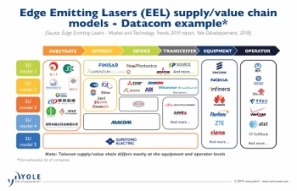
Specifically, what can the datacom industry do to establish leadership in EEL? As per statistics, optical systems for datacom and telecom represent the largest EELs segment with 56 percent of the total revenue in 2018.
EEL vs. VCSEL
Finally, are VCSEL and GaAs potential application areas as well? Else, what’s different? Vallo said EEL is an edge-emitting laser diode and VCSEL is a surface-emitting laser diode. Both are photonic devices made of GaAs. The difference is in the way of output beam propagation (EEL – from the edge, VCSEL from the top) and thus, in the design.
Gallium arsenide (GaAs) is compound semiconductor material, used to epitaxially grow, particularly IR (infrared) and photonic devices (such as LED, EEL, VCSEL, etc.). Infrared (invisible) emission is given by the physical material properties of GaAs.
He added: “EEL and VCSEL are used in transceivers – optical modules installed in the datacenters. VCSEL-based transceivers are used for short transmission distances up to 300 m with lower transmission speed (< 5 Gbps) whereas EEL-based transceivers reach long-haul distances with high transmission speed (~ 40-50 Gbps).
“Moreover, both EEL and VCSEL are key devices that can be used for 3D sensing applications – LiDAR, face/gesture recognition. EEL is more powerful due to its higher intrinsic (natural) emission brightness, which helps to extend the sensing range.”
— By Aanchal Ghatak & Pradeep Chakraborty