


One of the largest obstacles limiting the next generation of computer chips may finally have a solution.
The shrinking of computer chips has exposed a stubborn problem: even when a semiconductor can carry electricity efficiently, getting that electricity into the material can waste power and slow the device down.
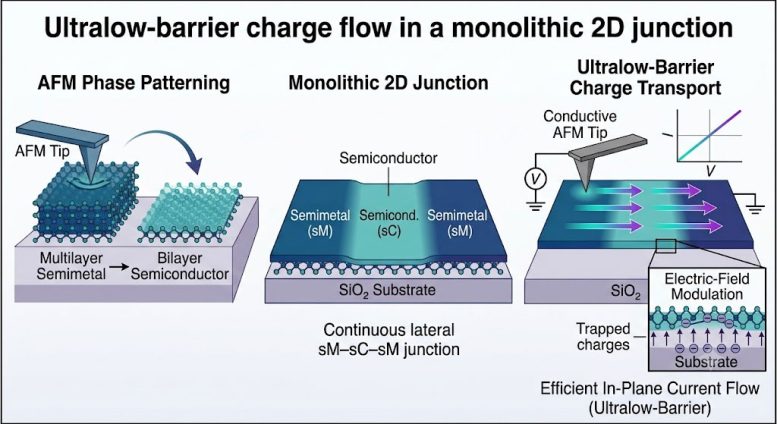
Researchers in South Korea have now demonstrated a possible way around this obstacle. Their design allows electrical current to move smoothly from a conductive region into a semiconducting region without crossing the conventional junction between two separate materials. The team also directly mapped the movement of charges at the nanometer scale, providing experimental evidence that the new interface does not disrupt the current.
The advance could support the development of smaller and more energy-efficient electronics, including AI processors, low-power devices, and future logic chips.
The research was led by Professor Seungbum Hong of KAIST’s Department of Materials Science and Engineering, in collaboration with Professor Kibum Kang at KAIST and Professor Sung Beom Cho’s team at Sungkyunkwan University.
Why Contact Resistance Holds Back Smaller Chips
Modern transistors depend on metal electrodes to deliver electricity into a semiconductor. However, the boundary where those materials meet can resist the movement of electrical charges. This contact resistance consumes energy, produces heat, and limits how much performance engineers can gain by making transistors smaller.
The problem is particularly important for two-dimensional semiconductors. These materials can be only one or a few atomic layers thick, making them attractive for electronics that may eventually need to operate at dimensions beyond the practical limits of conventional silicon. Yet their extreme thinness also makes it difficult to create efficient electrical contacts without damaging or altering the semiconductor.
Instead of placing a separate metal electrode on top of the semiconductor, the researchers created conductive and semiconducting regions inside one continuous sheet of platinum diselenide (PtSe₂).
Read the rest of the article from SciTechDaily here.