


By Layla Avagyan, Marketing Communications Specialist at HyePeak
Today, the electronics industry is experiencing rapid growth, with printed circuit boards (PCBs) seeing particularly high demand. Experts estimate the market will reach about USD 104.58 billion by 2030, up from USD 81.01 billion in 2025. However, this exponential growth poses significant environmental concerns, stemming from manufacturing processes, transportation, and other factors that impact ecology. For manufacturing companies, it becomes crucial to adopt sustainable practices. Central to this effort is the integration of Life Cycle Analysis (LCA) into PCB design and production.
In this article, we will explore the best practices for sustainability in PCB manufacturing, the role of LCA, its advantages, and the challenges faced along the way.
Environmental Risks of PCB Manufacturing

PCB manufacturing involves several processes that can pose significant risks to the environment if not properly managed. These include the use of hazardous chemicals such as etchants, solvents, and heavy metals, which can contaminate water, soil, and air when released into the environment. Additionally, waste materials and emissions from manufacturing plants can contribute to pollution and ecological imbalance.
To address these issues, manufacturers must adopt environmentally friendly materials and innovative processes such as lead-free soldering and non-toxic etching, which can significantly reduce ecological impact. Additionally, they should implement strict waste management protocols, ensure the proper disposal or recycling of hazardous chemicals, adopt cleaner production technologies, and incorporate Life Cycle Analysis (LCA) to continuously evaluate and minimize environmental impacts throughout the product’s lifecycle.
What is Life Cycle Analysis (LCA)?
Life Cycle Analysis (LCA) is a comprehensive method used to assess the environmental impacts associated with all stages of a product’s life – from raw material extraction to manufacturing, use, and end-of-life disposal or recycling. It provides a holistic view of a product’s environmental footprint, enabling designers and manufacturers to identify hotspots and opportunities for improvement.
In the context of PCBs, LCA considers factors such as raw material sourcing (metals like copper, gold, and rare earth elements), manufacturing energy consumption, transportation emissions, operational energy during device use, and disposal or recycling processes. Conducting an LCA helps stakeholders understand where environmental impacts are most significant and guides strategies to mitigate them.
LCA vs. Traditional Environmental Assessment
Traditional environmental assessments often focus on isolated aspects, such as energy use during manufacturing or waste generation at disposal. In contrast, LCA offers an integrated approach, capturing the cumulative environmental effects across the entire product lifecycle. This comprehensive perspective is crucial for PCBs, given their complex material composition and the multiple stages involved in their production and disposal.
Applying LCA to PCB Design
Material Selection
The foundation of sustainable PCB design begins with choosing environmentally friendly materials. For example, selecting lead-free solder and recyclable substrates reduces toxic waste and facilitates recycling at the end of the product’s life. Additionally, sourcing metals responsibly – such as recycled copper and gold – reduces mining impacts.
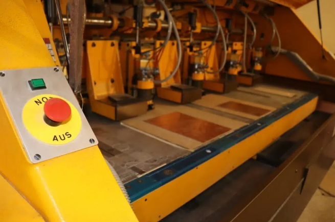
Manufacturing Processes
Manufacturing steps like drilling, plating, and soldering are energy and water-intensive. Optimizing these processes can lead to significant resource savings. For instance, reducing the number of layers and trace lengths minimizes copper and substrate use. Standardizing footprints and component sizes also streamlines fabrication, reducing waste and rework.
Design Considerations for Sustainability
Designing for durability extends the lifespan of PCBs, decreasing the need for replacements and reducing waste. Components rated for higher temperatures, moisture resistance, or vibration tolerance can withstand harsher conditions, limiting early failures. Incorporating effective thermal management and protective coatings also prolongs device life.
End-of-Life Management
PCBs often end up in landfills, where toxic metals and plastics can leach into the environment. Designing PCBs that are easier to recycle- such as using fewer composite materials or separating components into modules – facilitates efficient recovery of valuable materials and reduces environmental contamination.
Benefits and Challenges of LCA Integration
As the world increasingly prioritizes sustainability, businesses cannot afford to overlook their environmental impact. Investors, consumers, and regulators are demanding greater accountability, transparency, and demonstrable progress toward eco-friendly practices.
- Integrating LCA provides a strategic advantage by empowering organizations to create greener products, optimize resource efficiency, and minimize waste.
- LCA enables firms to develop and communicate credible environmental claims via Environmental Product Declarations (EPDs), which facilitate consumer comparison based on sustainability criteria. This transparency resonates strongly with the growing segment of eco-conscious consumers and investors, providing a competitive edge in an increasingly sustainability-driven market.
- LCA helps future-proof organizations against tightening environmental regulations, particularly those targeting waste management, carbon emissions, and resource conservation.
- Modern LCA tools and software streamline data collection, analysis, and reporting, making the methodology more accessible and accurate. As a result, organizations can embed sustainability into their innovation pipelines and product development workflows more seamlessly.
Challenges and the Future of LCA
Despite its clear benefits, conducting comprehensive LCA assessments remains complex and resource-intensive. Challenges include data variability, defining appropriate system boundaries, and dealing with subjective judgments in impact valuation. Gathering accurate, transparent data from suppliers and manufacturing processes can be difficult, especially in diversified or global supply chains.
However, as industries increasingly adopt LCA practices, technological advancements are alleviating some of these hurdles. Improved databases, standardized methodologies, and user-friendly software are enhancing the accuracy, consistency, and accessibility of LCA. Future developments aim to automate data collection through IoT sensors and integrate real-time environmental impact monitoring, making LCA a more dynamic and integral part of product lifecycle management.
Embracing sustainable practices through the integration of Life Cycle Analysis is no longer optional but essential for forward-thinking PCB manufacturers. Those that prioritize environmental accountability and transparency will not only meet the rising expectations of regulators, investors, and consumers but also set new standards for sustainability in the industry, ensuring positive societal impact.
Looking ahead, LCA will continue to evolve as a central tool in sustainable development, guiding innovation, regulatory compliance, and corporate responsibility. Its integration into broader sustainability frameworks – such as eco-design, circular economy models, and climate action strategies – will be essential for building resilient, environmentally responsible electronics industries.
Layla Avagyan is a Marketing Communications Specialist at HyePeak. An enthusiast in PCB design and electronics, Layla is passionate about sustainable engineering practices and innovative PCB solutions.