


Capturing the opportunities arising from the public and private investment in nearshoring semiconductor manufacturing has gone from a political football to a strategic imperative for companies looking for growth. But talk is cheap. How is the industry actually putting resources to work to build or expand the factories, address the technology challenges, and train the workers to achieve these capabilities across the globe in geographies that haven’t invested in these complicated activities in decades?
The associations are stepping up with new events and training programs. The software companies are building tools to address the training and supply chain challenges. New associations like PCBAA have formed to ensure the legislators understand how important it is to build out the entire electronics ecosystem, not just the chips.
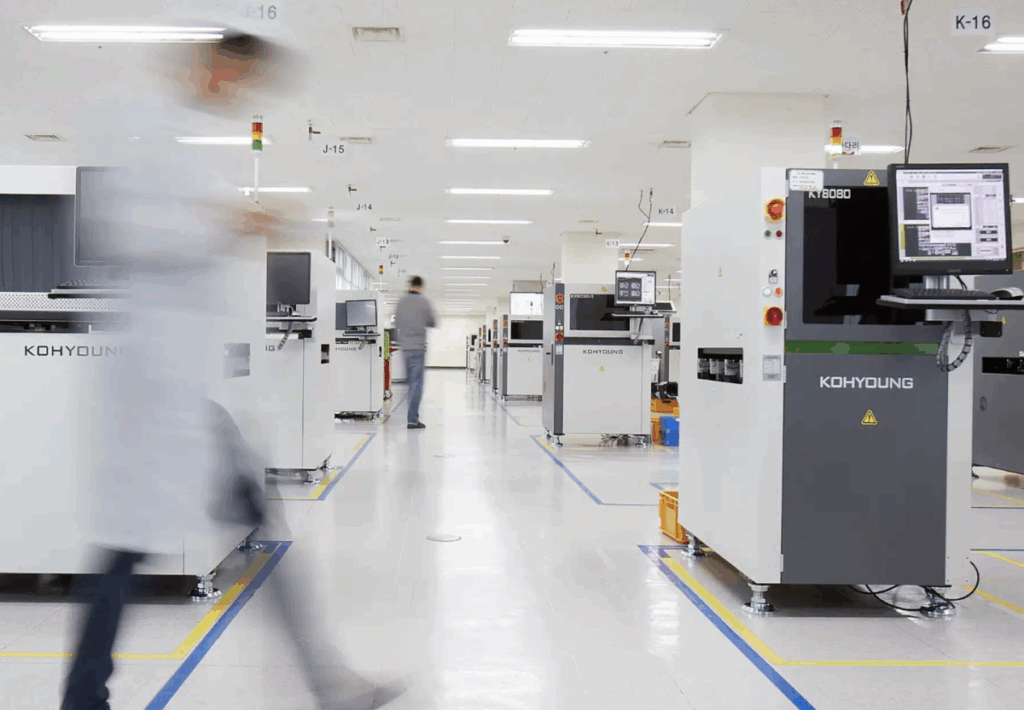
Equipment companies that have focused on SMT in geographies other than Asia are creating entirely new sales and marketing channels to reach an entirely new set of customers. We spoke with Brent A. Fischthal, Head of Global Marketing Communications at Koh Young Technology, Inc. to learn more about the details of bringing their inspection solutions, well received in Asia for these applications, into new geographies.

“The first thing we recognized is that the manufacturers’ rep network supporting our PCBA business is not ideally suited for semiconductor companies,” he explained. “The terminology, priorities, and success drivers in semiconductor and advanced packaging are quite different. For example, while PCBA has long acknowledged the limitations of 2D image matching as a primary inspection method, in the semiconductor arena, 2D has historically been the standard benchmark. Additionally, in this space, the conversation is not about inspection but about metrology and process control.
“So for the U.S. market, Koh Young partnered with NTV USA, a representative organization that focuses exclusively on semiconductor and advanced packaging customers in the United States. Their team brings the specialized expertise and relationships needed to effectively support this segment. This approach ensures that semiconductor manufacturers will have access to knowledgeable resources who understand their unique requirements and can clearly communicate the benefits of our 3D metrology solutions in a context that resonates with their process challenges,” he continued.
In an interview with EMSNOW, Koh Young’s Joel Scutchfield went into greater detail about how Koh Young’s inspection technology can be used in cleanroom and packaging processes. Watch entire video here.
“New partners like NTV USA can help us get access to this completely different customer base represented by the wafer fab manufacturers. They help us get access to this ’round world’ (as opposed to the ‘square’ SMT space) because that’s not where we traditionally go.”
EMSNOW talked to Joel right after IEEE’s Electronic Component Technology Conference (ECTC) in Dallas. “We were a prime sponsor of an event that gave us the opportunity to tell that group of high level executives about the solutions Koh Young can offer to these component manufacturers.”

Koh Young has developed the Meister Series and ZenStar, advanced metrology and inspection solutions tailored for the semiconductor industry. These systems are purpose-built to address the demanding requirements of advanced processes:
- Meister S: Designed for inspecting SiP and advanced packaging, the Meister S delivers high-precision 3D solder paste inspection with unparalleled accuracy and repeatability, ensuring superior control and yield optimization.
- Meister D: Built to inspect die and discrete components, the Meister D offers a specialized solution for ensuring product quality and reliability in high-volume semiconductor production environments.
- Meister D+: A dedicated inspection solution combining industry-leading Moiré technology and proprietary optics for highly reflective die applications, the Meister D+ provides capabilities for micro features.
- ZenStar: Koh Young’s wafer-level metrology solution, the ZenStar, delivers wafer metrology using proprietary deep learning technology to inspect defects such as micro-cracks, foreign material, chipping, and more.
Adapting to new markets is what world-class companies do. Koh Young intends to aggressively attack this space by listening to the customers and developing technology that doesn’t exist today for wafer-level manufacturing. According to Joel, Dr Koh is willing to devote the resources to not just succeed but dominate this market. We have no doubt he’s right and look forward to watching it happen.