


Atlanta, GA – Koh Young, the industry leader in True3D™ measurement-based inspection solutions, is pleased to announce its return to SEMICON West with a new series of inspection solutions designed to increase advanced package and semiconductor yield. Several of our latest inspection machines will be on display during SEMCION West in booth 329 from 11-13 July 2023 in the Moscone Center, San Francisco, CA.
The need for optical inspection in advanced package and semiconductor assembly arises from an increasing device complexity, high quality and reliability demands, process yield optimization, industry standard compliance, and cost reduction efforts. Wafer-Level Packaging (WLP), the technology of packaging a die while still on the wafer, is considered the next generation packaging technology, because it meets several of these criteria, yet many traditional inspection solutions fall short of delivering the capabilities required for success.
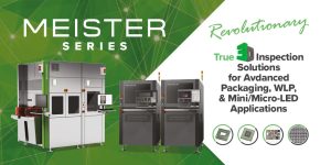
Building on our award-winning, industry-leading inspection technologies, the Koh Young Meister Series delivers True 3D measurement-based inspection for ultra-thin solder, wafer bumps, balls, and components. Manufacturers can maximize yield without increasing costs by detecting defects at the wafer level with accurate inspection.
Meister S Premium In-line 3D Inspection System for Micro Solder Paste Deposits
 Combining innovative vision algorithms and high-resolution optic technology, the Meister S is the ultimate, True 3D SPI solution for the semiconductor & Mini/Micro-LED packaging process improvement. ▪ High-resolution optics with a high-speed camera system (0.1 µm Z resolution)
· High-speed 25 Mega-pixel Camera with 3.5-micron Resolution Optics
· 10-micron Thins Solder Paste Inspection
· Colored and Transparent Flux Inspection
Meister D+ Breakthrough in 3D Measurement for Highly Reflective and Mirror-surfaced Components
The Meister D+ combines industry-leading Moiré technology to inspect for micro cracks, chipping, foreign material, and more and our new proprietary optics to support highly-reflective die inspection, a challenge historically plaguing the industry.
· Small Die and Component Inspection (0201 metric / 008004 EIA)
· Narrow-gap Inspection down to 50-microns
· True 3D Height and Tilt Measurement in High Density, Highly Reflective Applications
Meister W+ True 3D Measurement for Wafer Bumps & Shiny Components
Combining innovative vision algorithms and high-resolution optical technology, the Meister W+ inspects highly reflective die as well as components. With proprietary deep learning technology, it offers enhanced capabilities to inspect defects like micro-cracks, foreign material, chipping, and more.
· Industry-leading True 3D measurement capabilities enhanced by proprietary deep learning technology
· 10-micron diameter wafer bump inspection
· Revolutionary full 3D height and tilt measurement capability for even highly reflective die surfaces
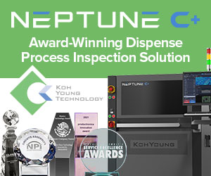
Neptune C+ Award-winning True3D Underfill and Coating Inspection with Thickness Measurement
Using UV light for presence or localized thickness inspection inherently limits accuracy, and applying a traditional laser approach is all too localized and simply takes too long in a production environment. Plus, these options only provide 2D results. The revolutionary Neptune C+ provides the ultimate solution to these and more challenges.
· L.I.F.T. (Laser Interferometry for Fluid Tomography) for non-destructive inspection
· True3D measurement-based Profiling of wet or cured materials
· Measures coatings, underfill, epoxy, bonding, glue, and more
If you cannot attend, you can still learn more about our best-in-class inspection solutions at kohyoungamerica.com.