


The SEMICON West 2025 design program “The Convergence of Semiconductor Manufacturing and Design,” organized by the ESD Alliance (ESDA), a SEMI Technology Community, featured presentations about successful collaborations between the design and manufacturing markets.
The three-hour program in a packed conference room included plenty of great material that we’re using as the basis for a blog series that you will see over the next several months. I’m working on them now based on my conversations with four of the speakers where we discuss key drivers behind the need for collaboration and what’s ahead.
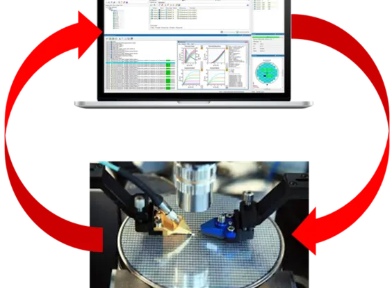
I’m starting with Dave Kelf, CEO of Breker Verification Systems, a company steeped in front-end chip verification, who describes an actual circular collaboration that effectively leverages AI and other electronic design automation (EDA) advances. We recently talked about collaboration, integrated design and manufacturing flows and AI.
Smith: How does Breker define collaboration between design and manufacturing?
Kelf: In general, at a technical level, we would define this collaboration as the sharing of data, methodology and/or information that improves both processes. As semiconductors become more complex, this sharing process is increasingly important to effectively manage the overall complexity of today’s chip designs.
Smith: What trends are driving the need for this collaboration?
Kelf: Apart from the ever-increasing size and density of semiconductors, there are specific trends that require more interaction between design, verification and manufacturing. Obvious developments include the advent of chiplets, given the changes in performance of signal paths, and 3D devices driving complex packaging, power dissipation and other issues. Design issues such as the increased need for SoC coherency testing and complex device structures such as multi-core processors, also play a role.
With many of these issues, design and verification (D/V) trade-offs have an impact on manufacturing, and vice versa. For example, differing delays on a Universal Chiplet Interconnect Express (UCIe) interface—an open specification for a die-to-die interconnect and serial bus between chiplets—will have an impact on hazard testing in coherency verification. As another example, thermal hotspots on some parts of a chip package might need additional testing during the verification phase.
Smith: What trends and challenges are preventing a fully integrated design and manufacturing design flow?
Kelf: Traditionally, the D/V and manufacturing teams have remained separate in most organizations, as well as between the two industries. EDA companies sell primarily to the design teams, although they do interact with the foundries at the back end of the process. Manufacturing companies work directly with different teams at the foundries and not with the D/V teams at all.
New relationships need to be built up. The general know-how in these disciplines is different, and methodology approaches tend to be disconnected. The tradition is to separate the processes and use standardized interfaces for communication that leaves little room for improvisation. All this needs to change so that teams can begin to work more closely.
Smith: What is circular EDA-manufacturing collaboration and vertical integration?
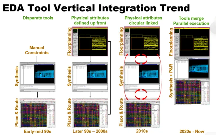 Kelf: In past EDA flows, we have seen disparate tools performing specific functions. As semiconductors got smaller, their physics changed and this led to the design process absorbing new characteristics. For example, abstract designs were run through synthesis to create gates connected by wires. This format was then passed to place and route (P&R) tools that would lay out the gates in terms of transistors and interconnects on the silicon wafer.
On large devices, the gate level signal delays were larger than the interconnect, allowing design to be separated from layout. As silicon became denser, the interconnect delays became the dominant factor, and the layout of the device impacted the design synthesis process. The two tools required forward integration—synthesis projected layout rules to P&R, and a reverse integration where layout characteristics were sent back to synthesis for redesign where required delays could not be handled during P&R.
The methodology went from a simple flow to a circular design approach as synthesis and P&R cooperated. The same is now true of design and manufacturing where solving the problems noted above requires this same circular cooperation.
Smith: What will it take to have an integrated design and manufacturing flow?
Kelf: A lot of cooperation between different groups. As we reach limits in areas such as signal integrity and thermal management that will squeeze silicon efficiency improvements, these methodology linkages will be required for continued progress and growth. The industry (both design and manufacturing) will be highly motivated to make this happen.
Smith: From a personnel perspective, who (on both sides) are the typical touchpoints?
Kelf: It will be the engineering staff from both the design side and manufacturing that work closely to develop technical solutions. Executive-level support is, of course, needed to cement the collaboration.
Smith: Where does AI fit?
Kelf: AI will have a role to play in this. Estimating the factors that drive efficient design to manufacturing to design flows is a critical step in speeding interaction and providing sensible estimated starting points. AI can process the large amounts of data necessary to provide these estimates as we now see complex chips that contain billions of transistors. AI will be needed to accelerate the interactions for different tools through the development process.
As design and manufacturing collaboration becomes a critically important industry strategy, companies are turning to SEMI and its Technical Communities such as the ESDA and their wide-ranging initiatives. For details and to get involved, visit the ESDA website at https://www.semi.org/en/communities/esda.
To learn more about Breker and its solutions that provide test content portability and reuse to solve complex semiconductor challenges across the functional verification process, go to: https://brekersystems.com.
About Dave Kelf
 Dave Kelf holds the position of CEO of Breker Verification after serving as its Chief Marketing Officer responsible for all aspects of Breker’s marketing activities, strategic programs and channel management.
Earlier, he served as vice president of worldwide marketing solutions at formal verification provider OneSpin Solutions, was president and CEO of Sigmatix, Inc., and held senior positions at Cadence, Synopsys and Springsoft. Kelf holds a Bachelor of Science degree in Electronic Computer Systems from the University of Salford and a Master of Science degree in Microelectronics from Brunel University, both in the U.K., and an MBA from Boston University.
Robert (Bob) Smith is executive director of the ESD Alliance, a SEMI Technology Community.