


By Scott Green, Principal Solutions Leader, 3D Systems
 We are all too familiar with the pandemic’s impacts – not the least of which is the blow dealt to supply chains and the global shortage of semiconductors. This is disrupting the production of many consumer products from cars to electronics, and the demand for microchips is greater than ever.
If we need more chips, can’t chip manufacturers just increase manufacturing capacity? In theory, it sounds easy, but production capacity and technology are challenging that intent.
For fabs to increase production, they need to install new manufacturing lines. They require new equipment, and capital equipment manufacturers are innovating to help fabs meet the increased demand. However, these tools are complex and expensive with a long product development cycle with lead times up to nine months. It is difficult for capital equipment manufacturers to pivot their production lines that rely on traditional manufacturing technologies, and scale to meet unexpected demand growth.
Accelerating Innovation with Additive Manufacturing
Traditional manufacturing workflows are hampered by several limitations. If a capital equipment manufacturer needs to surge order a part, it may require more resources than one supplier can handle. The overhead required to set up an additional supplier is prohibitive. Additionally, with the desire to create and deliver more productive equipment more quickly, traditional product development workflows are lengthy and cumbersome due to the need for tooling.
Additive manufacturing (AM) removes these limitations, enabling freedom of design, and a seamless transition from prototyping to low volume production of bespoke parts. When capital equipment manufacturers integrate AM into their traditional manufacturing workflows, it is possible to optimize strength-to-weight ratios, integrate conformal cooling structures, and reduce system part counts and the need for assemblies. This results in improved fluid dynamics, reduced assembly failures, better kinematics, and closer adherence to theoretical operation states. With hundreds of thousands of components required to create a tool, the options for which applications can be improved via AM seem limitless. Three in particular have demonstrated advantages.
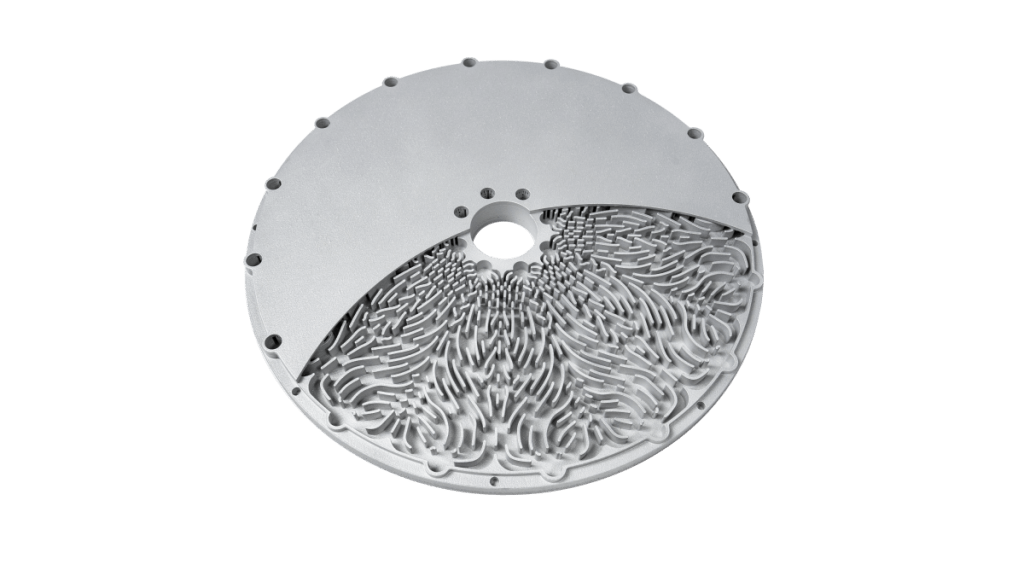
Wafer Table Thermal Management

Better thermal management of critical semiconductor equipment components, such as wafer tables, can improve semiconductor equipment accuracy by 1–2 nm and simultaneously improve speed and throughput. Increased machine speed and uptime leads to more wafers processed and higher overall lifecycle value.
During lithography, keeping temperatures within milliKelvin (mK) ranges is critical as any system disturbance has an impact at the nanometer scale. Through design for additive manufacturing (DfAM), it’s possible to optimize internal cooling channels and surface patterns, thus dramatically improving surface temperatures and thermal gradients while reducing time constants. With unique designs attainable with AM, it is possible to efficiently dissipate heat, enhance system throughput and accuracy, and improve overall performance. A large semiconductor capital equipment manufacturer using AM to produce their wafer tables realized an 83% decrease in ΔT (13.8 to 2.3 mK), and a 5x reduction in time to wafer stabilization.Another benefit of using AM to produce wafer tables is structural optimization and tables with reduced part counts and assemblies. Producing parts using traditional technologies relies on brazing to join parts together. Brazing is a lengthy, low-yield process with a 50% rejection rate which renders it inefficient when rapid iteration is desired. Replacing multipart assemblies with monolithic additively manufactured parts increases reliability, improves manufacturing yield, and reduces labor costs.
Manifold Fluid Flow Optimization
Using traditional manufacturing processes to produce complex fluid manifolds results in large, heavy parts that have non-optimal fluid flow due to abrupt transitions between components, and channels with sharp angles that lead to disturbance, pressure drops, stagnant zones, and leakage.
When AM is employed to produce these same manifolds, engineers can optimize their designs to reduce pressure drop, mechanical disturbances, and vibration. A 90% reduction in flow-induced disturbance forces reduces system vibration and realizes a 1–2 nm accuracy improvement.
Structural Optimization & Advanced Flexures
AM gives designers the flexibility to optimize the structural topology of a part (i.e., lightweighting) with a suite of high-strength metal alloys. These designs can more precisely meet the performance requirements of semiconductor capital equipment, improve the strength-to-weight ratio, and deliver a faster time to market. Lightweighting semiconductor components and advanced motion mechanisms reduces inertia and improves lithography and wafer processing machine speed and uptime, leading to more wafers processed. In one example, a semiconductor capital equipment manufacturer was able to employ AM to achieve greater than 50% weight reduction in flexures, 23% higher resonant frequency, and reduced system vibration.
The Opportunity is Limitless
AM in the semiconductor space has not been addressed frequently, which leaves many to wonder if this is a widely embraced technology in the chip industry and where it is making an impact. AM – specifically direct metal printing – is a recognized, validated technology in the semiconductor capital equipment industry. The pressures within the market for optimization, the demand for more equipment, and the production barriers are requiring a rapid movement towards additive. Wafer processing equipment is currently in development – and some even shipping – that include additively manufactured parts.
From a lithography perspective, a large volume of equipment is already being used in production to create chips using a ~14nm process. AM can affect this existing install base by OEMs creating field upgrades to improve aspects of those systems. However, this is less likely a significantly enabling pathway. A more likely scenario is that AM will significantly enable newer machines that are either shipping today or will be shipping in the next one to two years. With this runway, there is ample time for component and system level redesigns which will increase productivity and quality. Additionally, the manufacturers will still have enough control over those systems to rigorously test and prove performance gains.
Outside of lithography, there are dozens of other applications in the process chain such as polishing, light sources and etching, sorting, and even metrology. The expanded use of AM in this segment is coming at a perfect time as equipment manufacturers are speeding towards some ‘cliffs of impossibility’ where physics will inevitably create limitations that are extremely challenging to overcome. In this realm, additive manufacturing will more likely enable and unlock new process levels. It won’t be able to eliminate the barriers of physics and the eventuality of some massive shifts in process. However, it is sending those challenges decades into the future, and allowing semiconductor capital equipment manufacturers to rethink what is possible and push the boundaries. In so doing, there is a tremendous opportunity for AM to be an important technology to overcome the semiconductor shortage, and once again strengthen supply chains.
Scott Green is Principal Solutions Leader at 3D Systems focused on helping semiconductor capital equipment manufacturers redefine their processes through the integration of additive manufacturing. He joined the company in 2012 and has held leadership roles in both sales and product management. Scott holds a Bachelor of Science in Electrical Engineering from the University of Maryland, and has studied Bioengineering at Stanford University.