


By Robert (Bob) Smith is executive director of the ESD Alliance, a SEMI Technology Community
Presentations from SEMICON West’s “The Convergence of Semiconductor Manufacturing and Design” offer great insights into the collaboration between the two, as I was recently reminded by presenter Sutirtha Kabir, R&D Engineering, Executive Director at Synopsys.
Reviewing his talk “Revolutionizing Silicon to Systems Design: Unlocking the Future with 2.5D and 3D Multi-Die Innovations” was a good kick-off for our discussion that covered the continuous need for collaboration and where AI fits. Kabir, as I quickly learned, is a technical innovator and articulate communicator passionate about ongoing collaborations between design and manufacturing.
This SEMI blog post is the second in a four-part series featuring presentations from the SEMICON West design program, organized by the ESD Alliance, a SEMI Technology Community. The first blog, with Dave Kelf, CEO of Breker Verification Systems, appeared on January 6 (“Circular Collaboration Leverages EDA Advances”).
Smith: How do you define collaboration between design and manufacturing?
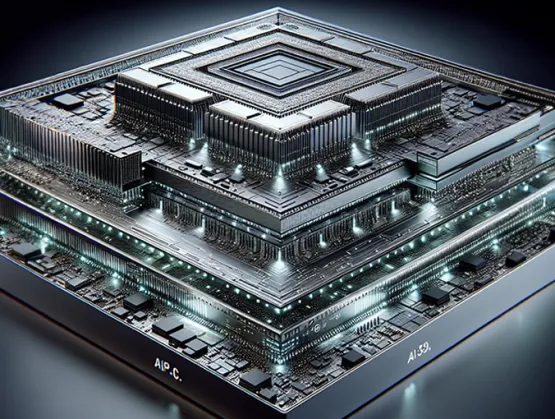
Kabir: Multi-die design and advanced packaging are a big focus of high-performance computing (HPC) and AI chips. Engineers are trailblazing and foundries are coming up with new stacking combinations. For this reason, design and manufacturing teams need to be closer than ever. Solutions must be made available to give ample visibility to manufacturing from the very start of the design process.
Single die design has been done for 15 to 20 years with a continuity of power, area, and performance (PPA). Design flows, methodologies and the ecosystem between design houses, EDA vendors and foundries are mature and stable. The conundrum is that it’s a different situation with multi-die designs. Not only is multi-die emerging rapidly, but the types of design innovations are different.
We have been working closely with our foundry partners to move multi-die innovation forward by enabling more advanced process and packaging technologies. I don’t see this slowing down as they are coming up with different ways of doing designs. Design teams are collaborating closely with the foundries to take advantage of the benefits of these new multi-die designs.
Smith: You mentioned new stacking combinations and collaboration with the foundries. What about collaboration with the OSATs?
Kabir: Generally, it’s both silicon foundries and OSATs. With advanced packaging, both play a significant role depending on the types of applications being targeted. Design house targets may shift from the traditional silicon foundry to several OSATs. For example, if an organic interposer is required, the collaboration could be with an OSAT in conjunction with the silicon foundry. There are many possible collaborations that may be required.
The point I’m trying to make is that there is a strong need for collaboration between EDA and the foundries during design that continues through manufacturing and test.
Smith: What trends in general are driving the need for this collaboration?
Kabir: The trends are performance and scalability and the need for high-performance compute. Look at some of the mega-chip systems coming out today compared to the bigger systems from five years ago. HPC was not driving that much in 2.5D. The big interposers used to be on silicon, maybe 1.2 to somewhere around less than three reticle sizes. Today, the reticle limit is more than 5X.
Leapfrog to today, and the configuration has changed where the state of the art is to use an organic interposer with multiple embedded bridges (up to 20 or more) buried inside the interposer to support high-speed interconnect. The organic interposer with multiple layers on the front side and back side communicates with bridges and the SoC and HBM that sit on top of that interposer.
3D architectures stack dies with GPUs and a large amount of HBM such as an HBM4 memory stack. The memory stacks may be 8 or 16 high. All of this memory needs to be as close as possible to compute for scalability. In terms of the high-power demand, the designer needs to make sure that the voltage that is pushed from the bottom of the stack can feed the power hungry SoC blocks on top of the 3D stack.
At the end of the day, EDA is all about giving design and manufacturing houses the capability to predict how a design is going to perform in all different kinds of scenarios. EDA must keep up with this trend and that requires collaboration.
Smith: What about the verification side, specifically system verification?
Kabir: Let’s say I am using a spreadsheet and doing back-of-the-napkin calculations, a technique that used to work well for single die or design blocks. Multi-die doesn’t scale since multiple heterogeneous dies in a single package must be considered. Design planning must include directional changes to measure the effects with key performance indicators. The challenge is to correlate signoff and verification. Signoff engineers can no longer just verify at the end of the design cycle. Instead, it has become a continuous process that transcends the flow from design planning through implementation and signoff and release to manufacturing.
The industry is repeating a pattern from about 20 years ago, when single-die design evolved from relatively naive approaches to much more sophisticated EDA-flow-driven methodologies.
Smith: As you drive the tools forward, who are your counterparts on the manufacturing side?
Kabir: It depends on the different stages of design—design planning, implementation or signoff. It starts at the architecture stage from the left when architects and physical design engineers are doing floorplanning. The term design technological co-optimization (DTCO) has evolved into S (system)TCO now because we are trying to co-optimize system design and technology.
I’ll give you a simple example. A working chip manufactured in a certain technology node is going to be used in a multi-die design. Is the existing chip technology good enough to support the design or will it require a new chip at a different node? In either case, how does an engineer work with the manufacturing house to make sure it has the right metal layers or a different number of metal layers or a different metal width or some other property on the technology side? Designers need to make data-driven decisions based on the configuration and technology numbers to meet power budgets.
In the past, what was once managed through designer-ASIC house-manufacturing interactions are now increasingly being handled by EDA flows as part of design implementation.
Smith: Ultimately, it’s driven by business. The hard work and decisions are made by two teams of knowledgeable technical people who must come together.
Kabir: And then of course it has to be rolled into program management, business development and all this needs to be supported by data. We all recognize that the design window is not increasing. It’s always about trying to get more out in less time with less people. That doesn’t help the equation.
Bob Smith: How does AI fit into this and how is it best leveraged?
Kabir: I’m hearing, learning, and reading about the tremendous advantages AI could bring. AI has a huge role to play, but it won’t eliminate the need for savvy design and verification engineers.
Multi-die design brings together different users from different tool backgrounds. Even the language between a packaging person and a silicon person is different. The terminologies they use are different, as are the ways they have done design over the last 15-20 years. The same applies to thermal, power or signal integrity engineering. Bringing them together requires that EDA will provide platforms where the whole system design, including chip design, is managed.
That’s a tall ask for people from all different backgrounds to come in, learn different technologies and tools within a short time. This is where ChatGPT or Microsoft’s Co-Pilot can be applied in the EDA world today to quickly find solutions by reading through manuals, application notes, forums and the like to find solutions. This use of AI agents can save tremendous amounts of time for designers.
Another aspect that can be positively impacted are roles. We have customers coming to us and brainstorming on the use of workflows and methodologies, instead of the design aspect. Scalability from the human perspective has become difficult because of the need to closely guide engineers to get them up to speed on new technologies and workflows. This is where Agentic AI can deliver a huge productivity boost. It’s not replacing anyone. It’s getting them to decisions and end results faster.
Smith: Can Agentic AI play a big role?
Kabir: Current AI is like the person who, when asked a question, has to give an answer even if it’s the wrong answer. The same thing is going to happen when we bring in all these EDA technologies with AI capabilities.
The point I’m trying to make is how do we verify that AI is doing the right thing? In EDA, one of the biggest questions and concerns is if a result or outcome or design can be verified. If it can’t be verified accurately, verification engineers will not trust what AI is telling them no matter how fantastic the algorithm is. The verifiability of AI solutions is important for EDA. The key question is: Why would I trust what your tool is telling me to do?
EDA flows that are more mature rely on decades of expertise, thorough documentation, and various scenarios to train AI algorithms. Those are the AI-powered EDA flows that I trust the most.